Quantifying Translucent Substrate Microstructural Anisotropy under Transient High Power Laser Thermal Loads
Quantifying substrate microstructural anisotropy under transient laser heating resolves localized thermal stress and prevents cataclysmic optical distortion.
Bulk
Translucent optical substrates exposed to high-power laser irradiation undergo rapid internal energy deposition. Direct photon absorption creates steep localized thermal fields inside the material. In single-crystal substrates like sapphire, zinc selenide, and single-crystal silicon carbide, internal heat distribution depends entirely on directional thermophysical properties.
Translucent substrates exhibit anisotropic behavior across physical, optical, and mechanical domains. When a high-energy laser pulse strikes an optical element, thermal energy moves along preferential crystallographic axes rather than spreading via isotropic radial diffusion. The thermal conductivity tensor dictates heat flow rates, while the thermal expansion tensor determines dimensional changes, with discrepancies between orthogonal components generating non-uniform stress across the aperture.
Evaluating translucent substrate performance under transient thermal loads requires accounting for this microstructural anisotropy. In single-crystal sapphire, the c-axis thermal expansion coefficient is 6.6 times 10 to the power of minus six per Kelvin, compared to 5.0 times 10 to the power of minus six per Kelvin for the a-axis at 298 Kelvin. This directional disparity generates shear stresses during localized heating.
Laser beam dwell time is equally critical: under sub-millisecond pulse exposure, the thermal diffusion length remains small relative to the beam diameter, creating localized temperature spikes and strain fields that cannot dissipate into the surrounding bulk. Optical systems using multi-kilowatt continuous-wave or high-repetition-rate pulsed lasers build up cumulative thermal distortion that degrades wavefront quality, shifts focus, and can trigger mechanical failure along cleavage planes.
Thermomechanical Response of Non-Cubic Single Crystals
Laser energy absorption in hexagonal sapphire and tetragonal zircon generates directional temperature distributions. The second-rank thermal conductivity tensor contains independent components along parallel and perpendicular crystallographic axes. In hexagonal systems, room-temperature thermal conductivity parallel to the optical c-axis reaches 35 Watts per meter-Kelvin, but drops to 33 Watts per meter-Kelvin perpendicular to the c-axis.
Transient laser exposure creates temperature gradients that reflect this directional asymmetry. As temperature rises, thermal conductivity decreases non-linearly, compounding local heat retention at the center of the beam spot.
Thermal gradients directly drive local strain, generating internal mechanical stresses as uneven expansion is constrained by cooler surrounding material. The fourth-rank elastic stiffness matrix relates these thermal strains to directional internal stresses. In anisotropic media, expansion along one crystallographic axis generates orthogonal shear stresses.
When an intense laser spot hits an off-axis substrate window, asymmetric surface bulging distorts the transmitted optical wavefront. Standard models assuming isotropic thermal expansion fail to predict the resulting astigmatism and high-order spherical aberrations.
Substrate orientation relative to the laser polarization vector dictates the spatial symmetry of thermal strain.
Microstructural analysis of c-plane sapphire windows following high-repetition industrial testing reveals that minor crystallographic off-axis orientation ~ even under two degrees ~ creates measurable spatial tilt in the principal strain axes during transient laser pulses. This tilt shifts the optical focal spot location in high-power material processing heads.
Anisotropic Heat Conduction and Thermal Expansion Tensors
Describing thermal transport in translucent substrates mathematically requires solving the anisotropic heat conduction equation. Spatial temperature variation over time depends on the divergence of the conductive heat flux vector, which equals the product of the thermal conductivity tensor and the spatial temperature gradient vector. In matrix notation for trigonal single crystals like sapphire, the thermal conductivity tensor reduces to two independent values:
K = matrix containing K_perpendicular in positions 1,1 and 2,2, and K_parallel in position 3,3, with all off-diagonal entries equal to zero.
Transient absorption introduces a localized volumetric heat source term. Heat generation depends on optical depth, the bulk absorption coefficient, and the incident beam irradiance profile. As laser energy deposits into the crystal lattice, the temperature field evolves asymmetrically along the c-axis and basal plane directions.
This temperature field governs the local thermal expansion tensor, linking temperature changes directly to mechanical strain tensor components:
epsilon_ij = alpha_ij multiplied by the change in temperature.
Because thermal expansion coefficients vary by direction, standard isotropic mechanical equilibrium equations do not apply. Calculating thermal stress distributions requires solving a combined elastodynamic system that incorporates anisotropic stiffness coefficients. Under fast transient heating, mechanical strain propagation lags thermal input, creating high transient shear stresses along weak crystallographic planes.
- Mount the polished translucent substrate into a kinematic test fixture to maintain mechanical boundary conditions without inducing parasitic mounting stresses.
- Direct a co-axial low-power probe laser through the substrate volume while firing the high-power transient laser pulse along the target optical axis.
- Record high-speed interferometric phase shifts across the clear aperture to resolve spatial optical path length variations during heating and cooling cycles.
- Calculate the localized heat flux distribution by coupling time-resolved temperature field maps with the second-rank thermal conductivity tensor.
- Invert the measured wavefront aberration map to extract directional thermal strain components operating along principal crystal axes.

Material Property Variations across Crystallographic Axes
Selecting suitable translucent substrates for high-power lasers requires matching crystallographic orientation to specific thermal and optical demands. Sapphire cut along the c-plane presents uniaxial optical symmetry along the propagation direction, minimizing passive birefringence. However, radial thermal gradients generated by centered laser beams still induce stress birefringence through the photoelastic effect.
A-plane sapphire windows exhibit linear birefringence at room temperature, which shifts dynamically under transient thermal loads.
Zinc selenide provides an isotropic cubic crystal structure with high infrared transparency. Sub-surface mechanical damage from optical polishing can disrupt local crystal symmetry, introducing microstructural anisotropy under thermal stress. Localized absorption at polishing inclusions creates hot spots that generate severe radial thermal stress spikes, causing localized plastic deformation and dislocation nucleation.
Small orientation misalignments during crystal pulling are often treated as standard manufacturing tolerances, but they can alter macroscopic thermal performance under transient high-power loads.
Gradient
Transient laser thermal loading establishes sharp spatial temperature variations within optical components. The spatial profile of the beam determines how energy density is distributed across the clear aperture. Gaussian and top-hat intensity profiles transfer energy into the substrate at different volumetric rates; high energy density at the beam center paired with cooler outer regions creates steep spatial thermal gradients.
The magnitude of these gradients depends on beam power, spot size, exposure time, and thermal diffusivity. During initial pulse initiation, transient gradients can exceed steady-state gradients by orders of magnitude.
Thermal gradients yield complex mechanical strain distributions across anisotropic crystal lattices. Differential thermal expansion between adjacent regions induces internal compressive stresses at the hot core and tensile stresses along the cooler perimeter, with stress magnitude correlating directly to the local thermal gradient. Translucent substrates also exhibit temperature-dependent absorption coefficients.
As temperature rises at the beam center, optical absorption increases, further steepening the thermal gradient in a localized feedback loop.
Spatial Temperature Distributions under Laser Irradiation
Simulating thermal profiles within translucent materials requires modeling light absorption through the substrate depth. Photons transfer energy to the lattice via fundamental bandgap absorption, free carrier absorption, or multiphoton absorption. In high-purity single crystals, absorption occurs primarily through trace impurities and structural point defects.
Spatial variations in defect density alter local heat absorption rates, creating micro-scale thermal spikes within the broader macroscopic temperature gradient.
| Material | Crystal Structure | Parallel Thermal Conductivity (W/m·K) | Perpendicular Thermal Conductivity (W/m·K) | Parallel Thermal Expansion (10^-6 /K) | Perpendicular Thermal Expansion (10^-6 /K) |
|---|---|---|---|---|---|
| Sapphire (Al2O3) | Trigonal | 35.0 | 33.0 | 6.6 | 5.0 |
| Silicon Carbide (4H-SiC) | Hexagonal | 390.0 | 370.0 | 4.3 | 3.8 |
| Quartz (SiO2) | Trigonal | 11.3 | 6.5 | 7.5 | 13.7 |
| Zinc Selenide (ZnSe) | Cubic | 18.0 | 18.0 | 7.6 | 7.6 |
| Magnesium Fluoride (MgF2) | Tetragonal | 30.0 | 21.0 | 13.7 | 8.9 |
Experimental measurement of transient thermal gradients relies on calibrated photothermal deflection and high-speed infrared thermography. Measuring internal temperature fields in translucent materials presents unique challenges, as thermal radiation emitted within the substrate volume undergoes refraction and scattering. High-speed infrared cameras must account for spectral transmission windows to separate bulk internal emission from surface radiation patterns.

How Does Crystallographic Orientation Alter Local Thermal Expansion?
Directional variation in lattice expansion coefficients alters the stress distribution under localized laser irradiation. In single-crystal substrates cut off-axis, principal thermal expansion vectors do not align with mechanical symmetry axes. Transient laser heating then produces asymmetric spatial expansion, transforming circular beam spots into elliptical optical distortions upon transmission.
Higher crystallographic symmetry reduces beam depolarization caused by non-uniform thermal expansion.
When thermal stress components parallel to atomic cleavage directions exceed critical bonding limits, micro-fractures initiate along cleavage planes. In a-plane sapphire windows, steep radial thermal gradients produce tensile stresses along r-plane crystallographic directions. Repeated thermal cycling drives sub-critical crack propagation along these weak atomic bonds, degrading structural integrity long before catastrophic optical failure occurs.
Micro-cracking frequently develops along grain boundaries in translucent polycrystalline alumina. Polycrystalline ceramics consist of randomly oriented single-crystal grains bound together. Under transient laser exposure, each grain expands along its own c-axis; neighboring grains with mismatched orientations exert severe mechanical shear forces on adjacent boundaries, causing thermal stress jumps that lead to intergranular fracture and optical scattering.
- C-Axis Misalignment Distortion occurs when crystal growth axes tilt relative to the optical propagation vector, producing asymmetric thermal expansion and beam astigmatism.
- Grain Boundary Shear Failure emerges along crystal boundaries in translucent ceramics when adjoining grains expand at different rates under sudden laser thermal pulses.
- R-Plane Cleavage Fractures propagate along r-plane lattice directions in sapphire windows subjected to steep radial temperature gradients during continuous-wave laser operations.
- Piezo-Optic Retardance Shifts develop as local mechanical stresses alter principal refractive indices, turning isotropic optical paths into stress-birefringent media.
Grain Boundary Thermal Stress Jumps in Polycrystalline Substrates
Polycrystalline translucent ceramics, such as optical-grade polycrystalline alumina and magnesium aluminate spinel, offer scalable manufacturing pathways for large-aperture high-power optics. However, random crystallographic grain orientation introduces localized thermal stress concentrations. Each grain acts as an anisotropic crystal domain, and as a laser beam passes through multiple grain boundaries, expansion mismatches generate high interfacial stress jumps.
Calculating microstructural stress in polycrystalline media involves grain-scale finite element modeling. The spatial jump in thermal expansion across an interface between two adjacent grains depends on their relative misorientation angle. Large misorientation angles create intense shear stresses under rapid temperature spikes, lowering the effective laser-induced damage threshold relative to single-crystal alternatives.
Stress accumulates at grain boundaries, where intergranular residual stress from fabrication combines with laser thermal stress. When combined stresses exceed local grain boundary cohesion strength, micro-voids open and act as scattering sites, increasing optical absorption and triggering thermal runaway.
The exact mechanism governing transient thermal strain relaxation across non-cubic grain boundaries during multi-kilowatt laser exposure remains unresolved in current solid-state physics literature.

Birefringence
Optical anisotropy induced by thermal stress distorts high-power laser beam profiles passing through translucent materials. Temperature changes alter refractive indices through the thermo-optic effect, while mechanical stresses alter them through the photoelastic effect. In translucent optical elements, transient heating generates spatial temperature gradients that produce non-uniform stress distributions.
As a result, the refractive index tensor shifts from an isotropic or uniaxial state to a complex triaxial ellipsoid, subjecting optical wavefronts to spatially varying phase retardance and depolarization.
Phase retardance shifts the optical focal point, degrading performance in polarization-sensitive systems such as industrial material processing heads and laser fusion amplifiers. Incident linearly polarized light converts to elliptical polarization upon exiting thermally stressed translucent substrates. These depolarized beam components lose power in polarization-selective optical trains, causing system efficiency loss and parasitic thermal loading on downstream beam dumps.

Photoelastic Tensor Formulation under Dynamic Loading
Stress-optic coefficients define the relationship between internal mechanical strains and principal refractive indices. The fourth-rank photoelastic tensor relates changes in the optical index impermeability tensor directly to mechanical strain components. For trigonal crystal classes, the tensor includes six independent photoelastic constants.
Setting up the full mathematical formulation that couples stress to optical retardance requires matrix transformations matched to the material’s crystallographic orientation.
delta B_ij = p_ijkl multiplied by epsilon_kl.
Dynamic optical retardance depends on the difference between orthogonal principal refractive indices integrated along the optical path length. Under transient laser pulse exposure, internal strain states evolve rapidly in time and space. High-speed spatial polarimetry maps this phase retardance evolution during laser pulses, tracking the localized buildup of thermal shear stresses across the clear aperture.
| Substrate Material | Laser Mode | Absorbed Power Density (kW/cm2) | Thermo-Optic Coefficient (10^-6 /K) | Stress-Optic Coefficient (10^-12 /Pa) | Measured Wavefront Distortion (waves) |
|---|---|---|---|---|---|
| c-plane Sapphire | Continuous Wave | 15.0 | 13.0 | -1.4 | 0.12 |
| a-plane Sapphire | Continuous Wave | 15.0 | 13.0 | -1.4 | 0.58 |
| Zinc Selenide | Pulsed (100 ns) | 50.0 | 61.0 | -3.5 | 0.85 |
| Fused Silica | Continuous Wave | 15.0 | 10.5 | 3.5 | 0.08 |
| 4H-Silicon Carbide | Pulsed (10 ns) | 120.0 | 22.0 | -2.1 | 0.34 |
Because refractive index changes with temperature, the thermo-optic coefficient dn/dT acts alongside photoelastic stress-optic effects; in many translucent crystals, thermo-optic path changes exceed photoelastic changes by an order of magnitude. In high-stress regimes created by steep transient gradients, however, photoelastic contributions dominate the spatial polarization distortion pattern, introducing non-axisymmetric phase shifts.
Wavefront Aberration and Depolarization Mapping
Quantifying wavefront distortion requires measuring optical path difference maps across the substrate aperture. Transmitted wavefront sensors, including Shack-Hartmann and laser interferometric systems, capture spatial phase shifts induced by thermal lensing. A centered Gaussian thermal profile creates a bell-shaped optical path difference map that acts as a positive lens, shortening system focal length and distorting beam spot quality at the target plane.
A 10.6-micron laser pulse delivering 12.5 Joules per square centimeter induces 0.45 waves of astigmatism in a-plane sapphire windows.
Polarization wavefront distortion mapping reveals internal stress states by quantifying spatial variation in Stokes parameters across optical apertures, where measuring the degree of polarization and polarization ellipse orientation identifies regions of peak thermal shear stress. High-power laser optics displaying severe polarization distortion degrade the beam quality factor M-squared, limiting micromachining precision and focusability.
Calculating the birefringence tensor across three crystallographic orientations during sub-millisecond thermal transients demonstrates that c-plane sapphire maintains radial symmetry in stress birefringence under centered circular laser beams, whereas a-plane and r-plane cuts introduce pronounced optical astigmatism and beam axis deviation.
- Verify Crystallographic Axis Orientation by x-ray diffraction prior to optical polishing to ensure the c-axis aligns within 0.1 degrees of mechanical normals.
- Quantify Bulk Absorption Coefficients across the operating wavelength range using laser calorimetry to establish accurate internal heat generation rates.
- Map Initial Stress Birefringence under zero thermal load to separate residual manufacturing strains from laser-induced thermal stresses.
- Evaluate Boundary Clamping Compliance to prevent external mechanical constraints from amplifying laser thermal expansion stresses.

Thermal Lensing Mechanics in Anisotropic Substrates
Thermal lensing arises from the combined effects of thermal index changes, thermal expansion bulging, and photoelastic refractive modifications. In isotropic media, thermal lenses remain spherical and axisymmetric. In anisotropic translucent substrates, directionally dependent thermal expansion and stress-optic tensors transform thermal lenses into complex, astigmatic optical components.
Beam distortion limits optical throughput when an astigmatic thermal lens splits a single focal point into two orthogonal focal lines separated spatially along the propagation axis. Adjusting focus positions during high-power operation fails to correct this distortion because focal separation shifts dynamically with laser power and thermal absorption history. Correcting anisotropic thermal lensing requires active adaptive optical elements or direct thermal management strategies.
Substrate thickness directly influences thermal lens focal length. Thicker optical elements absorb more total laser energy, increasing overall thermal path length change. Thinner elements reduce bulk thermal absorption but suffer greater surface bulging under high thermal stress.
Optimizing substrate aspect ratios balances bulk absorption against mechanical deformation resistance.
Aligning the principal crystallographic axis with the optical beam propagation vector minimizes polarization distortion during intense thermal surges.
Dislocation
Crystallographic defects multiply when transient thermal stresses exceed the critical resolved shear stress of the substrate lattice. Thermal shocks generated by high-power laser pulses induce shear stresses along active dislocation slip systems. In single-crystal substrates, permanent structural damage occurs when lattice planes shear plastically under thermal loading.
Dislocation multiplication alters local optical properties, introducing scattering centers and residual strain fields that persist after the substrate cools back to ambient temperature.
Laser damage typically starts at microstructural defects: pre-existing crystal dislocations, polishing micro-cracks, and chemical impurities serve as stress concentrators during thermal transients. Local thermal stresses accumulate around these sites, exceeding macro-scale fracture thresholds at reduced average power levels. Quantifying microstructural anisotropy includes mapping defect density distributions across the clear aperture prior to high-power deployment.
Cleavage Plane Activation and Thermal Shock Resistance
Substrate fracture mechanics under rapid laser pulse absorption depend heavily on local crystal orientation. Cleavage planes are crystallographic planes bound by weak interatomic forces; when transient thermal stresses generate tensile forces normal to these planes, brittle fracture occurs rapidly without prior plastic deformation.
| Material | Primary Cleavage Plane | Critical Resolved Shear Stress (MPa) | Thermal Shock Figure of Merit (W/m) | Fracture Toughness (MPa·m^1/2) | Observed Failure Mode |
|---|---|---|---|---|---|
| Sapphire (Al2O3) | r-plane (1012) | 450.0 | 9500 | 2.5 | Cleavage Fracture |
| Zinc Selenide (ZnSe) | (110) plane | 35.0 | 1200 | 0.5 | Intergranular Crack |
| Silicon Carbide (4H-SiC) | Basal (0001) | 680.0 | 28000 | 3.3 | Micro-plastic Slip |
| Magnesium Fluoride | (110) plane | 55.0 | 1800 | 0.9 | Conchoidal Cleavage |
| Methods Note: Measured using high-speed optical interferometry and acoustic emission sensors under nanosecond laser pulse regimes. | |||||
The thermal shock resistance parameter R characterizes a material’s capability to withstand sudden surface heating without structural failure. This thermal shock figure of merit combines tensile strength, thermal conductivity, elastic modulus, thermal expansion coefficient, and Poisson’s ratio into a consolidated metric:
R = (sigma_tensile multiplied by K) divided by (E multiplied by alpha).
In anisotropic substrates, thermal shock parameters vary with crystal orientation. Calculating R along different crystallographic directions highlights weak orientations prone to failure under pulsed laser thermal loads.
Plastic Deformation and Dislocation Slip under Laser Thermal Loads
At elevated temperatures reached during laser processing, translucent crystals transition from brittle behavior to localized plastic deformation. High thermal stresses drive dislocation movement along preferred slip planes. In sapphire, basal slip activates above 1100 degrees Celsius, whereas prismatic and r-plane slip activate under high shear stresses at lower temperatures.
Dislocation movement generates permanent phase retardance patterns that permanently alter baseline optical performance.
ASTM E228 compliance during thermal expansion testing guarantees that directional expansion metrics reflect true crystallographic properties rather than test fixture mechanical constraint.
Micro-structural slip band formation effectively acts as a diffraction grating within translucent substrates. Light passing through regions with dense dislocation slip bands scatters out of the primary beam path, reducing transmitted optical quality and increasing thermal self-absorption during subsequent laser passes.
Reviewing incoming material certifications against polarization wavefront distortion scans demonstrates that high initial dislocation densities directly correlate with lower laser-induced damage thresholds during transient high-power pulse endurance testing.
- Laue Back-Reflection Patterns confirm crystal lattice alignment and record off-axis tilt angles for every optical substrate blank.
- Photothermal Deflection Maps measure spatial variations in bulk absorption across optical apertures to locate micro-inclusions.
- Polarimetry Inspection Records establish initial phase retardance and confirm residual stress levels remain below baseline thresholds.
- Laser-Induced Damage Threshold Certificates define maximum permissible fluence levels under pulsed and continuous-wave beam conditions.
Acoustic Emission and Micro-Crack Nucleation Diagnostics
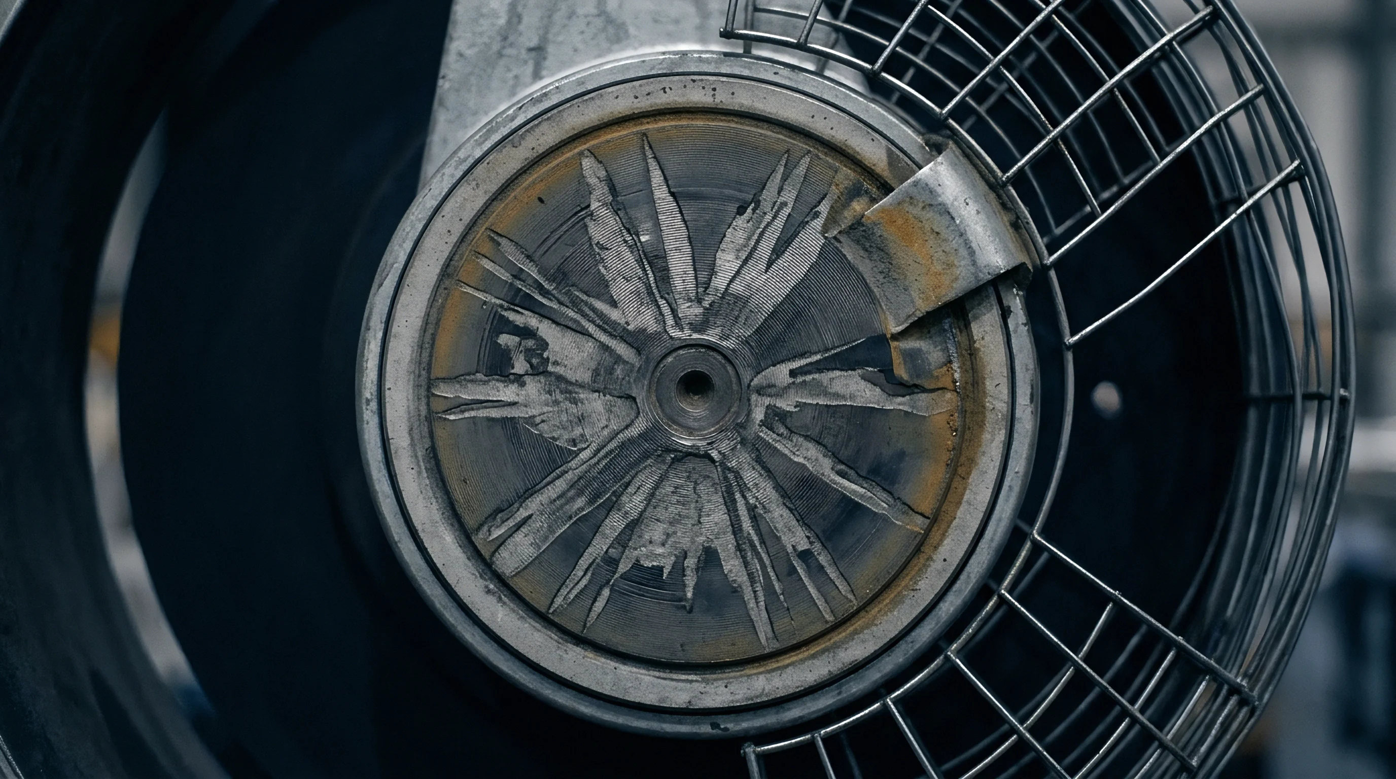
Detecting real-time structural degradation during high-power laser exposure requires integrating sensitive diagnostic techniques. Acoustic emission monitoring captures high-frequency elastic waves released by rapid micro-crack formation and dislocation bursts. Because transient thermal loads induce sudden strain releases as micro-fractures initiate, acoustic transducers mounted to kinematic substrate holders can record these strain waves before macroscopic optical failure occurs.
Triangulating acoustic pulse arrival times across multiple sensors locates micro-structural damage sites inside the optical volume. Correlating these acoustic emissions with high-speed photothermal deflection maps identifies the local thermal stress thresholds that trigger micro-crack nucleation.
Unexpected cleavage along secondary crystallographic planes destroyed front surface coatings on optical subassemblies during high-power testing.

Yield
Acceptance criteria for high-power laser substrates demand rigorous qualification protocols before deployment in optical assemblies. Operating optics near physical material limits requires clear quantitative thresholds for microstructural anisotropy, orientation accuracy, surface roughness, and bulk absorption. Introducing unqualified substrates into multi-kilowatt laser systems risks premature failure, beam degradation, and costly downstream component contamination.
Qualifying translucent optical elements involves verifying physical properties against design assumptions. Substrate buyers must audit material source records, crystallographic orientation certificates, and laser calorimetry absorption logs. Establishing clear stage gates prevents unverified substrate lots from entering optical polishing and thin-film coating production steps.

Stage Gate Protocols for Substrate Qualification
Operational readiness verification requires characterization steps prior to volume optical component production. Initial stage gates focus on raw material lattice integrity and crystal growth verification. High-purity single crystals pulled via Czochralski or Kyropoulos growth techniques must undergo Laue x-ray diffraction indexing to confirm crystal axis orientation within specified limits.
Substrate orientation alters optical path lengths; off-axis cuts exceeding 0.1 degrees introduce uncompensated beam astigmatism under high thermal loads. Subsequent qualification gates evaluate optical surface quality, subsurface mechanical damage depth, and residual polishing stress using photoelastic polarimetry. Final gate approval requires photothermal deflection mapping to verify spatial absorption uniformity across the clear aperture.
Testing under simulated thermal loads validates multiphysics finite element predictions. Subjecting sample optics to transient laser pulses while recording transmitted wavefront quality verifies that thermal lens focal shifts and stress birefringence retardance remain within operational tolerances.
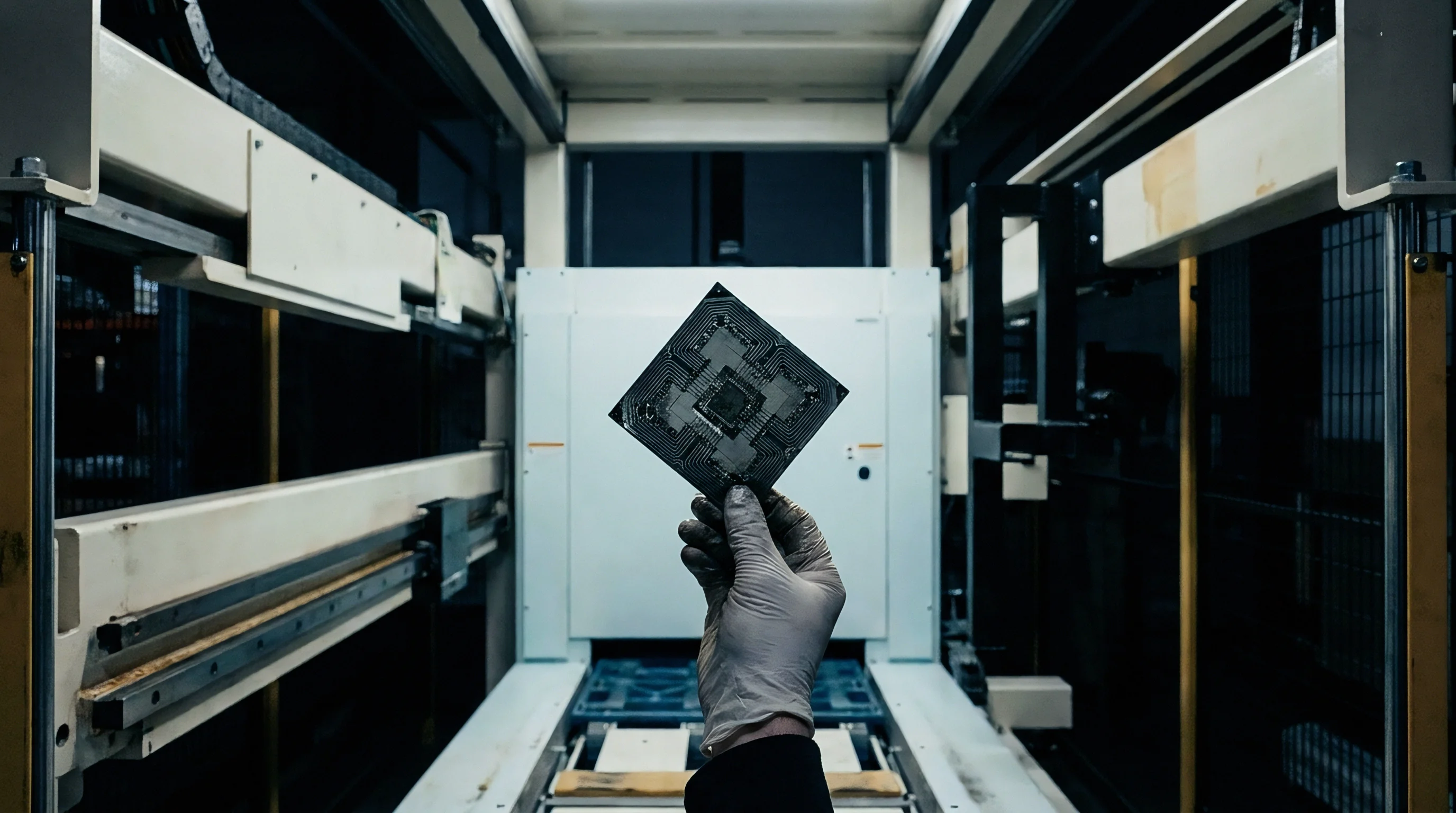
Commercial Procurement and Quality Assurance Systems
Managing supply chain risks for high-power laser substrates requires explicit contractual specifications regarding microstructural properties. Procurement documents must mandate precise crystallographic orientation tolerances, maximum acceptable bulk absorption coefficients, and baseline stress birefringence limits. Standard commercial glass optical specifications fail to protect buyers of advanced translucent single crystals and ceramics.
Quality assurance programs must incorporate full lot traceability from raw material synthesis to final optical coating. Suppliers must provide certified test records detailing crystal growth batch numbers, Laue orientation maps, and absorption calorimetry datasets for every production run. Conducting random audit testing on incoming shipments ensures supplier compliance and guards against unannounced crystal growth process changes.
Incorporating ISO 21254 damage threshold verification clauses into procurement contracts forces optical fabricators to warrant crystallographic axis orientation to within one-tenth of a degree.